Analysis Services
-
We established the analysis department to provide analysis services for semiconductor devices and quality control for CMOS-based fabrication processes. Over the years, the analysis services have been expanded and continued to offer services to local and overseas customers. Those services include the analysis of several kinds of materials, such as hard materials, metals, ceramics, polymers, rubber, and biological materials. In addition, Reverse Engineering (RE) technique developed and applied for various IC and MEMS devices. The RE technique is used for educational purpose and accomplished by taking an existing product and taking it apart to discover its internal structure and discover the technology involved in its fabrication. This huge evolution in the analysis department has been reached due to the possession of state-of-the-art analysis systems, enormous experiences owned by the analyst engineers, and their passion for gaining new experiences and knowledge.
-
The state-of-the-art analysis systems available in the analysis department include the following:
1. Sample preparation systems that include diamond scriber, ion sputter system, wet etching using chemical solutions, and dry etching using a plasma etch system.
2. Microscopic systems that include an optical microscope, Atomic Force Microscope (AFM), and Scanning Electron Microscope (SEM) equipped with EDX (Energy Dispersive X-ray) and FIB (Focused Ion Beam).
3. an advanced and sophisticated system like Micro System Analyzer (MSA) that is used to visualize and characterize the behavior of MEMS devices.
4. Experience in applying different microscopic analysis techniques that are used to reveal the topographical surface details, explore sample morphology, gain sub-surface information through cross-sectional samples and determine chemical elements that sample composed of.
-
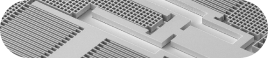 Electron microscope image of top-view sample that explores
the internal gyroscopic structure after applying the reverse
engineering technique on an existing device.
Electron microscope image of top-view sample that explores
the internal gyroscopic structure after applying the reverse
engineering technique on an existing device.
-
 Electron microscope image of cross-section sample that
explores the deep Si etch depth after applying the
cross-section analysis technique.
Electron microscope image of cross-section sample that
explores the deep Si etch depth after applying the
cross-section analysis technique.
-
 Electron microscope image of top-view sample that explores
the kinds of materials in the internal gyroscope structure
after applying the reverse engineering technique and the
mapping technique from the EDX system.
Electron microscope image of top-view sample that explores
the kinds of materials in the internal gyroscope structure
after applying the reverse engineering technique and the
mapping technique from the EDX system.
-
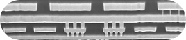 Electron microscope image of micro-cross-section sample that
explores the number of metallization layers in IC device
after applying FIB technique, wet etching, and RE
methodologies.
Electron microscope image of micro-cross-section sample that
explores the number of metallization layers in IC device
after applying FIB technique, wet etching, and RE
methodologies.
-
 Atomic Force Microscope (AFM) image that shows the
measurement of the stripes step height and the 3-D view of
the profile.
Atomic Force Microscope (AFM) image that shows the
measurement of the stripes step height and the 3-D view of
the profile.
-
 Electron microscope image of top-view sample that explores
the multi-level of metallization layers in NOR gate after
applying the de-processing analysis method and BSE detector.
Electron microscope image of top-view sample that explores
the multi-level of metallization layers in NOR gate after
applying the de-processing analysis method and BSE detector.
-
 Laser Doppler Vibrometer Polytec MSA explores the dynamic
visualization of out-of-plane Mode and corresponding
Frequency Response Function (FRF).
Laser Doppler Vibrometer Polytec MSA explores the dynamic
visualization of out-of-plane Mode and corresponding
Frequency Response Function (FRF).
-
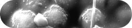 Electron microscope image of a top-view sample that explores
the shape of the internal structure of the powder sample by
using the SE detector.
Electron microscope image of a top-view sample that explores
the shape of the internal structure of the powder sample by
using the SE detector.
-
 Electron microscope image of top-view sample that explores
the different materials inside the internal structure of
tissue sample using BSE detector.
Electron microscope image of top-view sample that explores
the different materials inside the internal structure of
tissue sample using BSE detector.